For years, charge-couple device (CCD) sensors, known for their high-quality imaging capabilities, have been the gold standard in scientific instrumentation. However, recent advancements in complementary metal oxide semiconductor (CMOS) sensors have positioned them as a cost-effective and competitive alternative that is quickly gaining traction in the field. In this article, we delve into the strengths and applications of CCD and CMOS sensors, exploring how this shift in technology is reshaping the digital imaging landscape.
Although CCD sensors have historically dominated the scientific instrumentation market, recent advancements in CMOS technology have made it a viable alternative to CCD technology, with a more affordable price and lower energy requirements. Here, we explore the relative strengths and applications of both technologies.
Introduction
First invented in the 1960s, CCD sensors were preferred over CMOS sensors due to the lithography techniques available at the time, which limited CMOS development. For the next 25 years, CCD sensors had been the go-to, gold standard technology for enhanced imaging performance, capturing high-quality, low-noise images in applications across professional, medical, and scientific imaging. Indeed, early versions of CMOS image sensors could not compete with CCD technology and were not embraced commercially due to their poor performance relative to CCD sensors (Bigas et al. 2006). However, by steadily approaching the quality and capabilities of CCD sensors, improvements in CMOS technology have resulted in its growing popularity since the 1990s. Understanding the distinct differences between CCD and CMOS sensors is key when it comes to prioritizing for image quality, power consumption, and speed.
Structural Differences between CCD and CMOS Sensors
Both CCD and CMOS technologies involve metal oxide semiconductor sensors that convert light into electrons by capturing photons with thousands of photosites. These photosites collect photons as the image is being taken, storing them as electrical signals. The primary difference between CCD and CMOS technologies is related to how they generate an image from electrical signals, that is, the way they handle each pixel.
A CCD sensor is an analog device in which the sequential transfer of charge from one pixel to the next occurs across the sensor to the readout register. An external amplifier then converts the charge from each pixel to a voltage signal, which is in turn converted to digital data by an analog-to-digital converter (ADC). When photons are converted to electrical signals, the charge converted to voltage is passed through a limited number of nodes, so fewer amplifiers and ADCs are in action, thus reducing noise in the output image. This makes them especially effective in low-light environments, allowing for detailed image capture, a key advantage in fields in which precision is critical, such as astronomical imaging. However, this serial charge transfer process is slow and consumes power.
Unlike CCD sensors, each pixel in a CMOS sensor contains not only a photosite but also a small amplifier that converts the accumulated charge to a voltage signal within the pixel itself. This localized conversion, known as active pixel sensor (APS) architecture, allows each pixel to operate independently, which results in faster processing and higher frame rates than with CCDs. In some cases, each pixel also possesses an integrated ADC that converts analog voltage signals to digital signals at the pixel level, which contributes to high-speed readouts. This design, while efficient, tends to introduce noise.
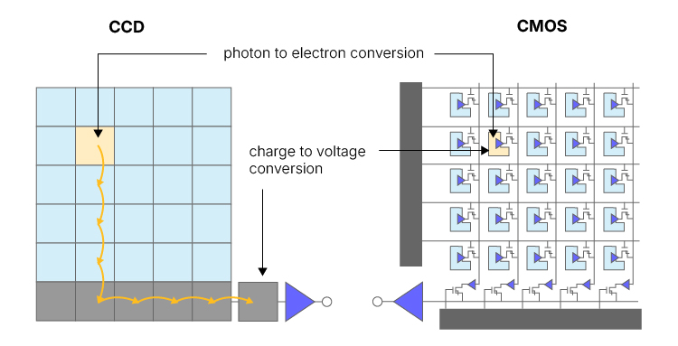
Charge-couple device (CCD) vs. complementary metal oxide semiconductor (CMOS) image conversion. CCDs move a photogenerated charge from pixel to pixel and convert it to voltage at an output node. CMOS imagers convert charge to voltage inside each pixel.
Manufacturing Processes and Cost
The manufacturing costs of CCD and CMOS sensors have changed over time, as influenced by technological advancements and industry needs. Initially, CCD sensors were the go-to for high-quality imaging, but their complex production processes, involving multiple photolithography and etching steps, made them costly to produce, with low yields. As a result, their utilization was primarily limited to high-end applications. In contrast, CMOS technology benefits from the use of established semiconductor manufacturing methods, which have already been optimized for cost efficiency. Overall, CMOS sensors are easier and more affordable to produce than CCD sensors, leading to increased process efficiency and low production costs. These cost differences have greatly impacted industry adoption, as large-scale operations now favor CMOS sensors for mass-market commercial applications.
Moving beyond CCD: Advancements in CMOS Technology for Scientific Imaging
As demand increases for CMOS sensors, research and development into CMOS technology is on the rise, whereas very little progress is taking place in the CCD arena. Advancements in CCD technology, such as improved charge-transfer efficiency and enhanced fabrication methods, have increased sensitivity and resolution while minimizing noise, and their leading status in applications requiring high fidelity, such as astronomy, has been maintained.
Nevertheless, recent advances in CMOS technology have led to the development of CMOS sensors of comparable imaging capabilities, and they are becoming increasingly popular in medical and scientific imaging applications. Moreover, innovations such as back-illuminated sensor (BIS) architecture and stacked sensor design have resulted in benefits such as CCD-like quantum efficiency and dynamic range while maintaining low read noise and high frame rates. As processing technology advances, CMOS sensors have become capable of additional functionalities such as hardware high dynamic range (HDR). Moreover, CMOS innovations allow for pixel-size adjustments, which further enhance image quality by accommodating more or larger pixels.
Overview of the key differences between CCD vs CMOS technology.
|
|
CCD Sensors |
CMOS Sensors |
Scientific Benefits |
|
Analog/digital |
Analog |
Digital |
Both methods are appropriate in scientific applications |
|
Structure |
Sequential pixel readout occurs via a single amplifier |
Each pixel has its own amplifier and operates individually |
CMOS increases the flexibility of binning options |
|
Quantum efficiency (sensitivity) |
High; excels in low-light conditions |
Comparable to CCD; enhanced with BIS technology |
Recent advancements in CMOS technology have significantly improved light capturing capabilities |
|
Image quality and noise |
CCD has historically been able to offer high-quality, low noise images |
Image quality is comparable to CCD due to advancements in CMOS technology |
Both methods are appropriate in scientific applications |
|
Speed and frame rates |
Readout speeds are slower due to sequential charge-transfer capabilities |
Processing is faster and frame rates are higher due to parallel pixel processing |
Both methods are appropriate in scientific applications |
|
Power efficiency |
Reliance on analog charge transfer leads to higher power consumption |
CMOS sensors consume up to 100 times less power than the equivalent CCD sensor |
Lower cooling requirements and operational efficiencies of CMOS sensors yield significant long-term energy savings |
|
Cost |
More expensive to produce |
Comparatively inexpensive to produce |
Significantly more development is taking place with CMOS sensors, offering continuous improvements in sensitivity as well as cost reductions |
BIS, back-illuminated sensor; CCD, charge-couple device; CMOS, complementary metal oxide semiconductor.
The Changing Face of Scientific Imaging: What Lies Ahead
The choice between CCD and CMOS sensors depends on the specific requirements of the application, balancing factors such as image quality, speed, power efficiency, and cost. Although once popular in scientific imaging, CCD sensors have been outpaced by developments in cost-effective CMOS sensors in the past few decades. As a result, CMOS sensors have gained traction in scientific instrumentation fields for applications such as fluorescence and super-resolution microscopy, histology imaging, and digital pathology.
Overall, as the quality of CMOS technology improves at a rapid rate, coupled with cost-effectiveness advantages, the adoption of CMOS in scientific instrumentation is likely to increase as CCD use declines. As we look to the future, ongoing innovation and research and development investments in CMOS indicate that it may not be long before CMOS becomes the technology of choice for life-science instruments, ultimately reshaping the landscape of scientific instrumentation.
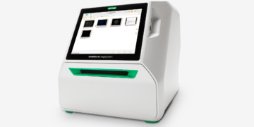
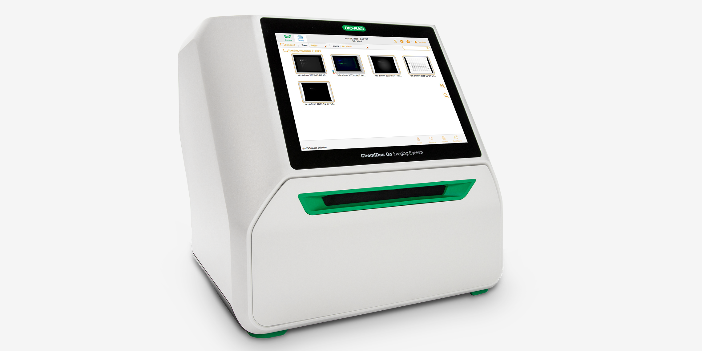
Bio-Rad is the first major life sciences company to provide the scientific instrument user with the option of CCD or CMOS technology in its range of digital imaging products for capturing gel and western blot images. The ChemiDoc Go Imaging System is the first in the Bio-Rad family of chemiluminescence-based digital imagers to incorporate advanced CMOS digital imaging technology.
As the transition from CCD to CMOS continues, researchers will benefit from greater flexibility, improved performance, and lower costs. With companies like Bio-Rad leading the way in providing both technologies, users can select the best imaging solution for their specific needs, ensuring that scientific imaging keeps pace with technological advancements.
References
Bigas M et al. (2006). Review of CMOS image sensors. Microelectronics Journal 37, 433-451.
Further Reading
CMOS Sensor Inc. (2024). CMOS vs CCD: A Review of Sensor Technology. https://www.csensor.com/ccd-vs-cmos, accessed March 18, 2025.
Edge AI and Vision Alliance (2023). CMOS vs CCD: Why CMOS Sensors are Ruling the World of Embedded Vision. https://www.edge-ai-vision.com/2023/04/cmos-vs-ccd-why-cmos-sensors-are-ruling-the-world-of-embedded-vision/, accessed March 18, 2025.
Kolabtree Blog (2022). Applications of CMOS in Medical Imaging and Life Sciences. https://www.kolabtree.com/blog/applications-of-cmos-in-medical-imaging-and-life-sciences/, accessed March 18, 2025.
Motras Scientific (2020). CCD vs CMOS – The Scientific Way. https://motras.in/2020/12/29/694/, accessed March 18, 2025.
Nevsemi.com (2024). CCD vs CMOS: Difference Between CCD and CMOS Image Sensor. https://www.nevsemi.com/blog/ccd-vs-cmos, accessed March 18, 2025.
New Scientific CMOS Cameras with Back-Illuminated Technology. Technical Notes. Teledyne Princeton Instruments. 2024. Available at: https://www.princetoninstruments.com/products/kuro-family/kuro/tech-notes/new-scientific-cmos-cameras-with-back-illuminated-technology, accessed March 18, 2025.
Oxford Instruments (2024). CCD vs sCMOS Cameras. https://andor.oxinst.com/learning/view/article/ccd-vs-scmos-cameras, accessed March 18, 2025.
Science Shot (2023). From Pixels to Pictures: Understanding CCD and CMOS Sensors. https://www.scienceshot.com/post/cmos-vs-ccd-who-is-the-clear-winner, accessed March 18, 2025.
Sorrel, C (2009). Inside the Nobel Prize: How a CCD Works. In Wired. https://www.wired.com/2009/10/ccd-inventors-awarded-nobel-prize-40-years-on/, accessed March 18, 2025.
SRI (2024). 75 Years of Innovation: CMOS, complementary metal-oxide-semiconductor. https://www.sri.com/press/story/75-years-of-innovation-cmos-complementary-metal-oxide-semiconductor/, accessed March 18, 2025.
Teledyne Vision Solutions (2024). CCD vs CMOS. Which is better? It’s complicated. https://www.teledynedalsa.com/en/learn/knowledge-center/ccd-vs-cmos/, accessed March 18, 2025.
Welover (2024). CCD vs CMOS Image Sensors: A Comprehensive Guide for Engineering Professionals. https://www.wevolver.com/article/ccd-vs-cmos-image-sensors, accessed March 18, 2025.